
Author Affiliations
Abstract
1 Centre for Optical and Electromagnetic Research, State Key Laboratory for Modern Optical Instrumentation, Zhejiang Provincial Key Laboratory for Sensing Technologies, Zhejiang University, Zijingang Campus, Hangzhou 310058, China
2 Imec USA, Nanoelectronics Design Center, Inc., 194 Neocity Way, Kissimmee, FL34744, USA
3 Ningbo Research Institute, Zhejiang University, Ningbo 315100, China
Chip-scale programmable optical signal processors are often used to flexibly manipulate the optical signals for satisfying the demands in various applications, such as lidar, radar, and artificial intelligence. Silicon photonics has unique advantages of ultra-high integration density as well as CMOS compatibility, and thus makes it possible to develop large-scale programmable optical signal processors. The challenge is the high silicon waveguides propagation losses and the high calibration complexity for all tuning elements due to the random phase errors. In this paper, we propose and demonstrate a programmable silicon photonic processor for the first time by introducing low-loss multimode photonic waveguide spirals and low-random-phase-error Mach-Zehnder switches. The present chip-scale programmable silicon photonic processor comprises a 1×4 variable power splitter based on cascaded Mach-Zehnder couplers (MZCs), four Ge/Si photodetectors, four channels of thermally-tunable optical delaylines. Each channel consists of a continuously-tuning phase shifter based on a waveguide spiral with a micro-heater and a digitally-tuning delayline realized with cascaded waveguide-spiral delaylines and MZSs for 5.68 ps time-delay step. Particularly, these waveguide spirals used here are designed to be as wide as 2 μm, enabling an ultralow propagation loss of 0.28 dB/cm. Meanwhile, these MZCs and MZSs are designed with 2-μm-wide arm waveguides, and thus the random phase errors in the MZC/MZS arms are negligible, in which case the calibration for these MZSs/MZCs becomes easy and furthermore the power consumption for compensating the phase errors can be reduced greatly. Finally, this programmable silicon photonic processor is demonstrated successfully to verify a number of distinctively different functionalities, including tunable time-delay, microwave photonic beamforming, arbitrary optical signal filtering, and arbitrary waveform generation.
silicon photonics programmable photonic integrated circuit waveguide delay lines Mach-Zehnder interferometer Opto-Electronic Advances
2023, 6(3): 220030

Author Affiliations
Abstract
1 Centre for Optical and Electromagnetic Research, State Key Laboratory for Modern Optical Instrumentation, Zhejiang Provincial Key Laboratory for Sensing Technologies, Zhejiang University, Zijingang Campus, Hangzhou 310058, China
2 Ningbo Research Institute, Zhejiang University, Ningbo 315100, China
3 imec USA, Nanoelectronics Design Center, Inc., Kissimmee, Florida 34744, USA
4 Ocean College, Zhejiang University, Zhoushan 316021, China
All-optical silicon-photonics-based LiDAR systems allow for desirable features in scanning resolution and speed, as well as leverage other advantages such as size, weight, and cost. Implementing optical circulators in silicon photonics enables bidirectional use of the light path for both transmitters and receivers, which simplifies the system configuration and thereby promises low system cost. In this work, to the best of our knowledge, we present the first experimental verification of all-passive silicon photonics conditional circulators for monostatic LiDAR systems using a nonlinear switch. The proposed silicon nonlinear interferometer is realized by controlling signal power distribution with power-splitting circuits, allowing the LiDAR transmitter and receiver to share the same optical path. Unlike the traditional concept requiring a permanent magnet, the present device is implemented by using common silicon photonic waveguides and a standard foundry-compatible fabrication process. With several additional phase shifters, the demonstrated device exhibits considerable flexibility using a single chip, which can be more attractive for integration with photodetector arrays in LiDAR systems.
Photonics Research
2022, 10(2): 02000426

Author Affiliations
Abstract
Hybrid integration of III–V and ferroelectric materials is being broadly adopted to enhance functionalities in silicon photonic integrated circuits (PICs). Bonding and transfer printing have been the popular approaches for integration of III–V gain media with silicon PICs. Similar approaches are also being considered for ferroelectrics to enable larger RF modulation bandwidths, higher linearity, lower optical loss integrated optical modulators on chip. In this paper, we review existing integration strategies of III–V materials and present a route towards hybrid integration of both III–V and ferroelectrics on the same chip. We show that adiabatic transformation of the optical mode between hybrid ferroelectric and silicon sections enables efficient transfer of optical modal energies for maximum overlap of the optical mode with the ferroelectric media, similar to approaches adopted to maximize optical overlap with the gain section, thereby reducing lasing thresholds for hybrid III–V integration with silicon PICs. Preliminary designs are presented to enable a foundry compatible hybrid integration route of diverse functionalities on silicon PICs.
Journal of Semiconductors
2021, 42(4): 041303
Author Affiliations
Abstract
1 Centre for Optical and Electromagnetic Research, State Key Laboratory for Modern Optical Instrumentation, Zhejiang Provincial Key Laboratory for Sensing Technologies, Zhejiang University, Hangzhou 310058, China
2 Institute of Port, Coastal and Offshore Engineering, Ocean College, Zhejiang University, Zhoushan 316021, China
3 Engineering Research Center of Oceanic Sensing Technology and Equipment, Ministry of Education, Zhejiang University, Hangzhou 310000, China
4 e-mail: leimeng.zhuang@ieee.org
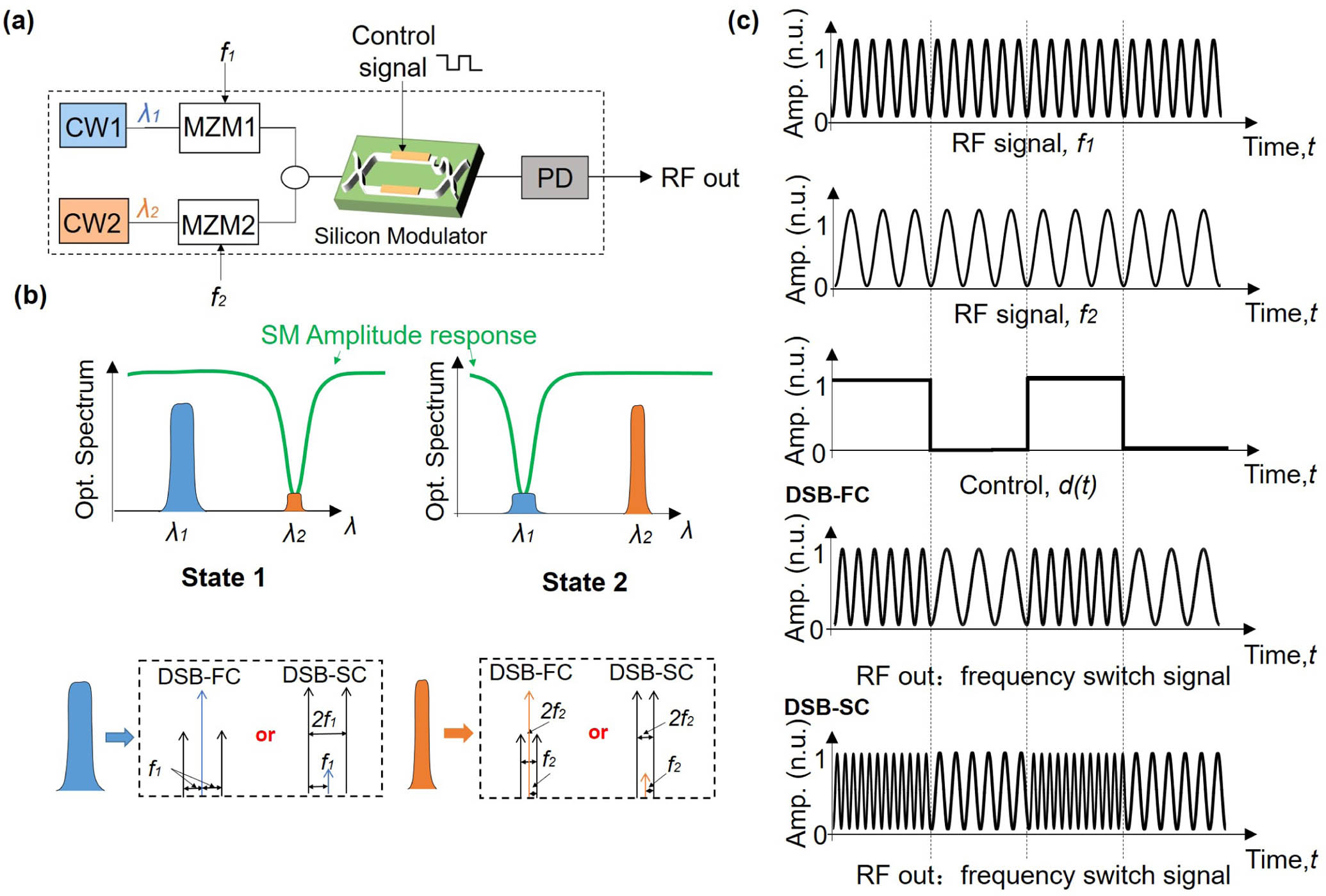
Radio frequency (RF) switches are essential for implementing routing of RF signals. However, the increasing demand for RF signal frequency and bandwidth is posing a challenge of switching speed to the conventional solutions, i.e., the capability of operating at a sub-nanosecond speed or faster. In addition, signal frequency reconfigurability is also a desirable feature to facilitate new innovations of flexible system functions. Utilizing microwave photonics as an alternative path, we present here a photonic implementation of an RF switch providing not only the capability of switching at a sub-nanosecond speed but also options of frequency doubling of the input RF signals, allowing for flexible output waveforms. The core device is a traveling-wave silicon modulator with a device size of and a modulation bandwidth of 10 GHz. Using microwave frequencies, i.e., 15 GHz and 20 GHz, as two simultaneous RF input signals, we experimentally demonstrated their amplitude and frequency switching as well as that of the doubled frequencies, i.e., 30 GHz and 40 GHz, at a switching frequency of 5 GHz. The results of this work point to a solution for creating high-speed RF switches with high compactness and flexibility.
Photonics Research
2020, 8(6): 06000852


